Four Things Every Engineer Should Know about PFAS
PFAS impacts on the semiconductor industry
What are PFAS chemicals?
“PFAS” is an acronym for pper- and polyfluoroalkyl substances. These man-made chemicals migrate into soil, water, and air when produced and used. There are many ways humans come in contact with PFAS, such as in non-stick cookware or cosmetics, but by far the most significant impact on human health is when PFAS is consumed in drinking water. Exposure to PFAS may result in a wide range of health problems, including cancer, liver disease, and immune system, thyroid, and developmental effects, according to Centers for Disease Control and Prevention .
The Environmental Working Group created an interactive map to understand the impact PFAS are having on wildlife and the environment. Their research showed that PFAS levels are so high in most freshwater fish that even infrequent consumption would increase the amount of PFAS in a person. Additionally, PFAS exposures have been linked to decreased hatching success in birds and sea turtles.
Since PFAS are bioaccumulative, meaning that organisms absorb the chemicals faster than they are excreted, it has become a growing concern to eliminate the exposure to PFAS as much as possible. The semiconductor supply chain is a contributor to PFAS in wastewater, according to the National Institute of Science and Technology (NIST).
How PFAS are used in the semiconductor industry?
PFAS have several unique chemical properties that make it appealing to semiconductor applications. Due to its chemical resistance, thermal stability, and hydrophobic (water repellant) properties, PFAS are utilized in various parts of the semiconductor manufacturing process.
Click the icons to understand the various semiconductor applications PFAS are used in. Recognizing where they are used is the first step to finding PFAS-free alternatives or adapting processes.
There is an industry-wide effort to eliminate the release of PFAS from all aspects of the semiconductor supply chain. Currently, the majority of Brewer Science’s BARC materials are PFAS-free. Although challenging, a relentless effort to eliminate PFAS from our product portfolio is underway. We are pursuing a multi-faceted approach to reduce and eliminate the lasting impact of forever chemicals within our materials by collaborating with our suppliers and local universities to synthesize PFAS-free additives, cooperating with SEMI and SIA focus groups, and reformulating our materials to remove these chemicals altogether.
Are there any regulations effecting the use of PFAS in semiconductor materials?
The Environmental Protection Agency (EPA) has set a Maximum Contaminant Level (MCL) for perfluorooctanoic acid (PFOA) and perfluorooctanesulfonic acid (PFOS) at 4 ppt. PFOA and PFOS are long-chain perfluorinated compounds, meaning that they have eight or more fully fluorinated carbon atoms; or six fully fluorinated carbons in regards to PFOS. Brewer Science has already eliminated PFOS and PFOA from our entire material portfolio, and we are working towards eliminating PFAS altogether by 2028.
In the United States, there are currently not any industry or national regulations on these PFAS analytes, however the Semiconductor PFAS Consortium tracks these in an effort to understand how these analytes are affecting our wastewaters.
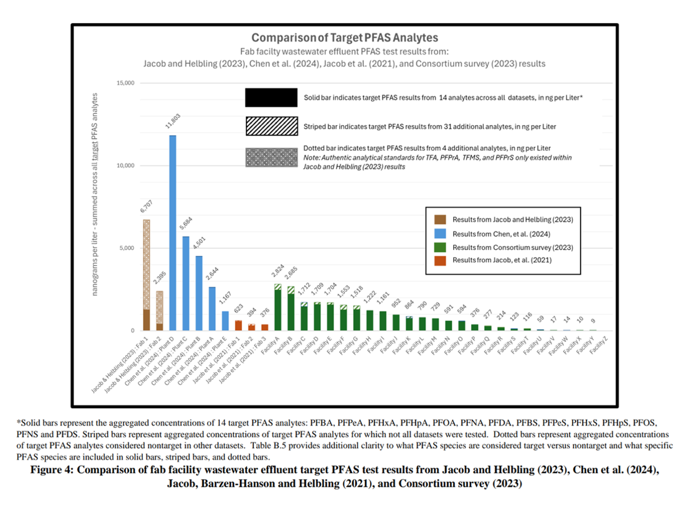
Image source: Semiconductor PFAS Consortium
The European Union is taking a more stringent approach to eliminating PFAS contaminants from their wastewater, and has proposed restrictions under Annex XVII, which targets specific PFAS subsets, including
- Perfluorocarboxylic acids (C9-C14 PFCAs)
- Perfluorohexane sulfonic acid (PFHxS)
- Undecafluorohexanoic acid (PFHxA)
Eliminating these three types of PFAS analytes will have an effect on photolithography patterning, etch precision, and adhesion. Overcoming this challenge requires a commitment to material innovation, focusing on the alternatives that have similar performance with different chemistries.
Why should the semiconductor supply chain work towards PFAS elimination?
“Current target PFAS analytical methods offered by commercial laboratories are incapable of characterizing certain other PFAS species potentially present in facility wastewater effluent. Additional research will be needed to develop a more complete understanding of semiconductor PFAS releases, the factors contributing to variations in the release of PFAS from semiconductor fabs, and potential measures to reduce or eliminate these discharges,” states David Isaacs, Vice President, Government Affairs of Semiconductor Industry Association in the article, Consortium Publishes Survey Results of PFAS Discharges to Wastewater.
The need to identify alternatives to PFAS is a growing concern. While there may not be strict guidelines or policies in place today, the desire to protect our planet and wastewater is a responsibility every fab should consider. As research and data is collected on fab contributions to PFAS in wastewater, policies could be enforced in the future, placing the semiconductor industry in a detrimental situation to find an alternative or risk process changes, therefore the need to innovate is today. Investing in PFAS replacement research and development today helps understand the role the analytes have in the process. Working cohesively with suppliers, customers, and the customer applications will help ensure the PFAS replacement alternatives provide a successful solution. It’s important to consider the implications of PFAS today and avoid the potential for technological setbacks that could hinder the ability to innovate.
PFAS-Free Bottom Antireflective Coatings
Currently, the majority of Brewer Science’s BARC materials are PFAS-free. With readily available i-Line, KrF, ArF, and EUV BARC and underlayer materials, we can find PFAS-free solutions suitable for your application. Additionally, Brewer Science has PFAS-free hardmask and spin-on-carbon materials, with a range of attributes including various levels of silicon content. Brewer Science recently launched a PFAS-free EUV ultrathin underlayer material.
PFAS-Free Advanced Packaging Materials
Brewer Science has several series of PFAS-free temporary bonding materials, including materials that work with chemical, mechanical, laser, and photonic debonding methods. Our BrewerBOND® VersaLayer system is an innovative solution for high-temperature and high-stress applications. For PFAS-free protective coatings specifically designed for wet-etch applications, look no further than Brewer Science® ProTEK® series materials.
To learn more about Brewer Science’s PFAS-free lithography materials or PFAS-free advanced packaging materials, submit a request at the bottom of this website.