Multi-Tier Die Stacking Enables Efficient Manufacturing
Achieve higher integration density with collective die-to-wafer bonding
Advanced packaging is currently facing a critical challenge to increase manufacturing efficiency without sacrificing device performance. Vertical integration techniques, such as multi-tier die stacking and hybrid bonding, enable increased integration density, therefore improving yield of high-quality devices. However, these highly precise processes require significant attention to defectivity, alignment, and scalability to ensure they achieve desirable yields and manufacturing efficiency.
Improving Yield through Minimizing Defects
Increasing yields in advanced packaging processes becomes more challenging in techniques that require a high-level of precision. Defectivity becomes a major concern, since the smallest variation or contaminant can render the device useless. This is why Brewer Science prioritizes proactive defect reduction through supply chain collaboration. While The Wall Street Journal states Brewer Science is a pioneer of perfection due to their zero-defect manufacturing process, the real challenge when it comes to advanced packaging is the ability to inspect die-level bonding surfaces prior to bonding.
In advanced multi-tier stacking, the ability to inspect surfaces on a die level prior to bonding can have a significant impact on yield by minimizing defects. Using Brewer Science’s materials, Koen Kennes at imec, a research and innovation hub in nanoelectronics, has proven high bond yields, close to 100% for N=2 stacks, and up to 90% for N=3 stacks.
Additionally, material selection must meet strict performance criteria while being compatible with high-throughput manufacturing. There are several important considerations to ensure the material can withstand high temperatures and offer efficient heat dissipation, which is essential as devices become more densely packed with components.
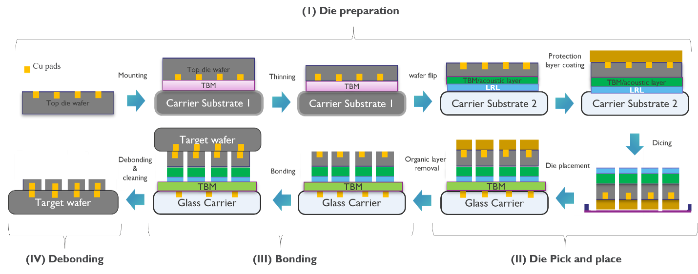
Caption: The collective-hybrid die-to-wafer bonding flow. After thinning on a temporary carrier, the laser release layer (blue layer) and acoustic layer (green) are introduced during the wafer flip to enable the coating of the protection layer (orange). After flipping the thin wafer on tape frame, the stack is singulated. Dies are picked up and place on a final temporary carrier where the dies are cleaned, bonded and debonded.
Credit: imec
Alignment
Maintaining precise alignment across multiple layers of stacked dies is critical for ensuring electrical connectivity and device performance. If dies are not aligned accurately, the interconnects, such as TSVs or microbumps, may not properly connect. This can result in open circuits or short circuits, ultimately leading to device failure.
Misalignment can cause increased resistance in electrical pathways, leading to high power consumption and excessive heat generation. This can reduce efficiency and reliability of the device.
Alignment accuracy typically within ± 2 micrometers for both N=2 and N=3 stacks is necessary. This precision is crucial for maintaining performance, particularly in applications requiring high-speed data transfer, such as HBM. The use of advanced tools for alignment and bonding ensures that even as the number of tiers increases, the performance is not compromised.
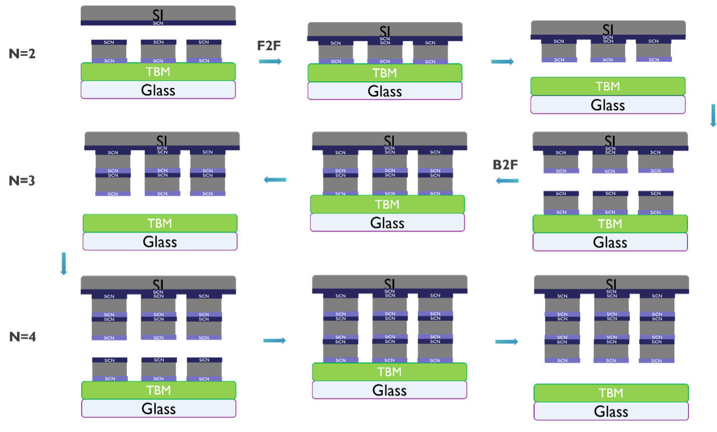
Caption: Simplified flow for N=2, N=3 and N=4 collective die-to-wafer transfer.
Credit: imec
Scalability
As packaging processes become more advanced, scaling them efficiently without sacrificing performance becomes more difficult. The inability to meet growing demand will result in loss of market share or missed opportunities in a growing market.
The multi-tier die stacking approach is scalable, allowing for the stacking of two, three, or even four dies in a single package. The collective die-to-wafer bonding process, despite being complex, is designed to be more efficient by allowing wafer-level processing. This reduces the need for individual die handling, which can be time-consuming and prone to contamination. The ability to process multiple dies simultaneously on the wafer level enhances manufacturing efficiency without compromising performance.
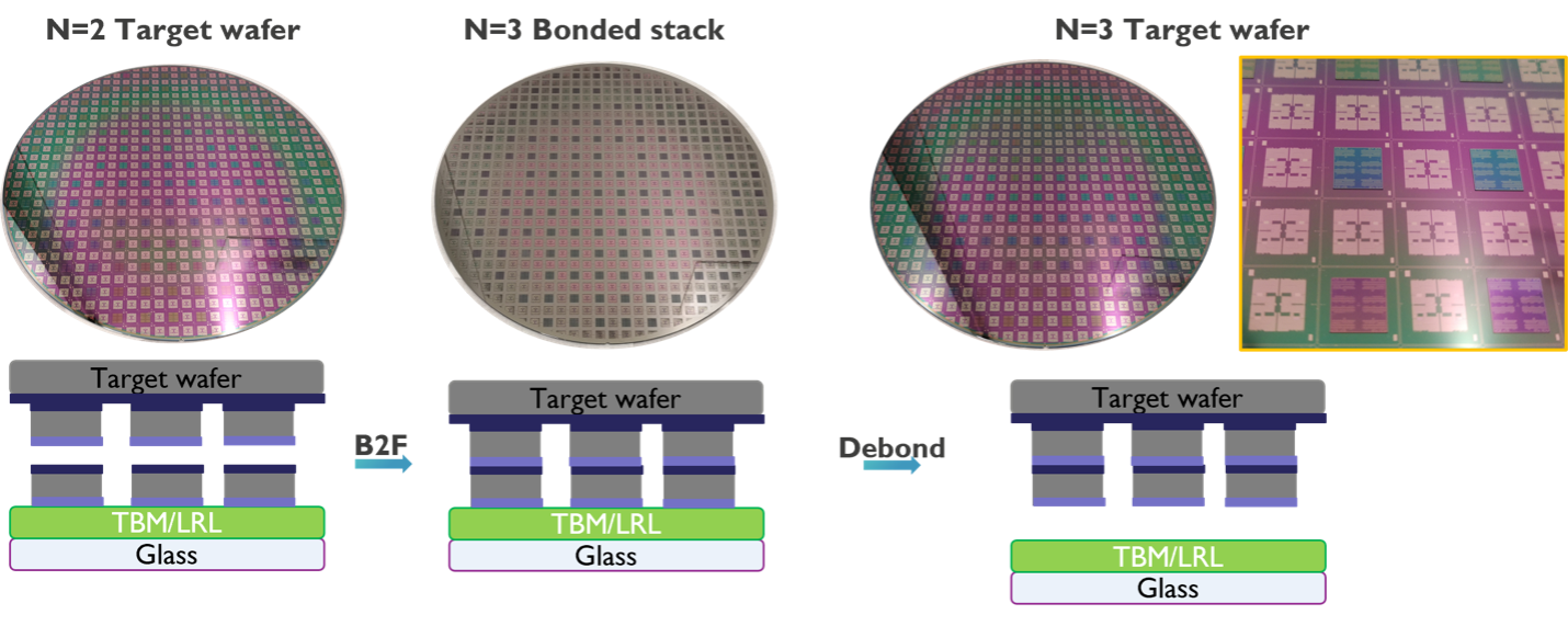
Caption: Simplified collective die-to-wafer bonding flow with pictures of the N=2 target wafer (after tier 1), the N=3 bonded stack and the N=3 target wafer (after tier 2).
Credit: imec
Multi-tier die stacking through collective die-to-wafer hybrid bonding presents a promising solution to many of the challenges faced by the advanced packaging industry. By enhancing integration density, maintaining high yields and precision, offering scalability, and improving manufacturing efficiency, this technology helps bridge the gap between the need for advanced device performance and the demands for efficient, high-yield manufacturing processes.
Download the White Paper for more detailed information.
The paper, “Multi-tier die stacking through collective die-to-wafer hybrid bonding”, explores the potential for collective die-to-wafer bonding to be successfully extended to enable multi-tier die stacking. As we move towards more complex IC designs, hybrid bonding will be a key enabler, allowing for efficient, high-density connections across multiple layers.


