Five Questions to Ask When Selecting a Temporary Bonding and Debonding System
Thin-wafer handling requires strategic material selection
High-bandwidth memory blocks (HBM) memory, microprocessors, field-programmable gate arrays (FPGA), AI accelerators, and other devices used in advanced system-level packaging all rely on temporary bonding and debonding systems to shrink their footprint. Understanding which properties play the most crucial role in device reliability and efficient production will ensure you are maximizing your yield, while reducing the device size. There are five questions you need to ask to ensure the solution you select for your temporary bonding and debonding system is best for long-term success.
What is the preferred debonding method?
Selection of the debonding method is highly dependent on a variety of factors, including desired throughput, capital investment, and cost of ownership. Debonding methods range from the relatively low capital investment of chemical release in a solvent bath to the higher capital investment of laser debonding with significantly increased throughput. Other debonding methods include thermal slide release and mechanical debonding. Each of the debonding methods has its own pros and cons, however, mechanical and laser debonding are the preferred methods for customers wanting to optimize throughput, minimize stress, and push the limits of wafer thinning.
(Click the tabs across the top of the image to compare release methods)
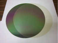
Picture illustrates laser debonding results at 308 nm using BrewerBOND® T1107 (2 µm) and BrewerBOND® C1301-50 (60 µm) materials, with 245 mJ/cm2 of laser fluence.
What are the thermal requirements?
As back-end-of-line (BEOL) processes become harsher, the need for a material set with higher mechanical, chemical, and thermal stability increases. In some cases, the specifics of the BEOL processing can require a material with mechanical, chemical, and thermal stability greater than what materials optimized for chemical and thermal slide debond methods can provide. When substrates have higher stress, room-temperature bonding with the appropriate materials can significantly reduce the bow and warp of the wafer stack. It also simplifies the process, therefore speeding up production cycles. This is particularly beneficial for advanced semiconductor devices that require precise and gentle handling. High-temperature bonding processes can cause thermal stress, slow down production and cause damage to delicate semiconductor structures.
For applications or downstream processes that require thermal stability up to 400°C without degradation or loss of mechanical stability, selection of the appropriate bonding material is critical.
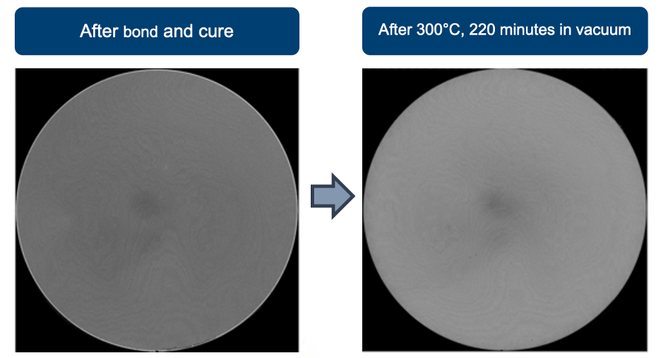
Picture illustrates bond line with BrewerBOND® VersaLayer™ materials survives 300°C for 220 mins (3 hours and 40 minutes) with no sign of decomposition.
Which topography does the material cover?
The necessity for a material to conformally coat the topography cannot be understated. In processes where copper pillars or solder bumps are used to form interconnects, the BrewerBOND® T1100 series material conformally coats the device features, while the BrewerBOND® C1300 series material, coated on the carrier wafer, embeds these features in the bond. The consequences of inadequate conformal coverage can lead to electrical failures, reduced thermal management, and reliability issues.
Achieving consistent and reliable bonds is critical for device performance. A high-flow, low-pressure curable layer is necessary to ensure strong adhesion without the risk of melt flow post-cure.
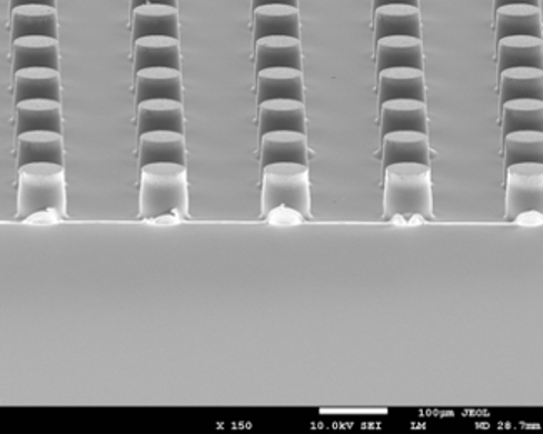 Image illustrates conformal coating on copper pillars
What are your adhesion requirements?
Strong bond line adhesion is necessary to prevent delamination. There is a delicate balance to ensure the adhesion is strong enough to keep the wafers bonded through processing while also ensuring a clean and controlled debond. One of the more common methods to quantify adhesion of bonded wafers is through the double cantilever beam test, which is also referred to as crack opening or razor blade insertion. With this method, a razor blade of defined thickness is inserted into the bond line a specified distance and the distance beyond the blade tip that the wafer pair delaminates after insertion is measured. In combination with the mechanical properties and thickness of the wafers, the surface energy of the bond interface can be calculated.
Strong substrate adhesion is important to ensure that delamination from the wafer pair during processing does not occur and that debonding happens at the proper interface.
A cross hatch test, more specifically ATSM D3359, is a standardized test to measure adhesion by tape. When a coating on silicon, silicon oxide (SiOx), or silicon nitride (SiNx) receives a 5B rating, it indicates that the adhesion between the coating and these specific substrates is of the highest quality. A 5B rating is specified as:
-
-
- No Peeling or Removal: The coating remains fully intact with no peeling or removal from the substrate after the tape is removed.
- Perfect Adhesion: The substrate and the coating have an excellent bond, ensuring the coating’s reliability and performance.
-
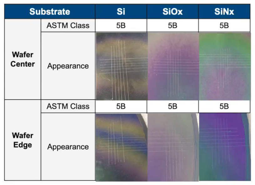 Chart illustrates Brewer Science’s Cross Hatch Test performed using its BrewerBOND® VersaLayer™ system materials.
What are the tolerances for thickness variation?
Total thickness variation (TTV) is a critical parameter that can significantly impact the uniformity, reliability, and performance of devices. In stacked applications, such as HBM and 3DIC, having a TTV that exceeds 5% could cause misalignment during die bonding and stacking. This can lead to poor electrical connections and mechanical instability. Additionally, TTV that exceeds 5% can lead to poor adhesion between the uneven surfaces, thus risking delamination and device failure.
Understanding the tolerance for TTV in your processes will ensure you have proper alignment and reliable connections, such as in stacked applications like HBM and 3DIC. TTV less than 5% is preferred for successful stacking and adhesion.
Brewer Science’s VersaLayer™ system is a set of materials composed of two BrewerBOND®materials. Together, these two layers enable mechanical stability with no movement and provide in-process thermal stability ≤ 400°C.
BrewerBOND® T1100 series materials are a thermoplastic platform applied to the device as a conformal adhesive coating.
BrewerBOND® C1300 series materials are a curable layer applied to the carrier that provides high-flow, low-temperature and low-pressure bonding with no melt flow post-cure.
The VersaLayer™ system materials are compatible with laser and mechanical debonding methods, offering versatility in your manufacturing process and requirements. Additionally, the total thickness variation is typically less than 5%.
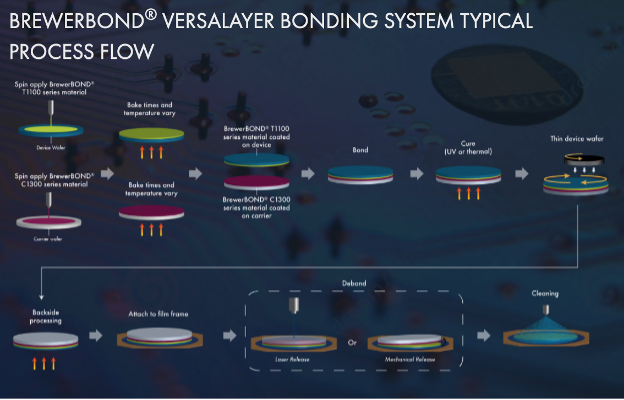 Illustrated is a BrewerBOND® VersaLayer™ system typical process flow. Modification may be necessary for specific applications.
The VersaLayer™ system successfully addresses the dual priorities of throughput and quality in semiconductor manufacturing. By enabling high processing speeds and room-temperature bonding, the VersaLayer™ system provides an efficient bonding processes. Simultaneously, its low warpage, thermal stability, precise bonding capabilities, yield improvement and flexible debonding methods ensure that the quality of the final products is not compromised. This balance makes the VersaLayer™ system an ideal solution for manufacturers looking to optimize both production efficiency and product excellence in the competitive semiconductor industry. Request more information on our Advanced Packaging webpage.