A high-level overview of wafer-level debonding options and considerations
As emerging technologies require ultrathinned device wafers, traditional debonding processes can pose some challenges. Photonic debonding is an innovative debonding process utilizing a carrier coated with an inorganic metal release layer that aids in the release of the thinned wafer from the carrier substrate with no force and no damage to the delicate wafer upon activation of the release layer by light. This debonding method is an alternative to processes that require more costly equipment and also suffer higher incidences of damage. After evaluating some of the traditional debonding processes in comparison to photonic debonding, some of the main advantages include carrier reuse, lower operational cost, less maintenance equipment and higher throughput.
There are many different ways to separate a thinned wafer from its temporary carrier substrate, also known as debonding. A critical challenge in this process is minimizing damage to the thinned wafers. Because each method has a different mechanism for debonding, it’s important to consider the application, material properties of the thinned wafer, and downstream processes. Click the icons to learn about the five most common debonding methods: thermal slide, mechanical debonding, chemical debonding, laser debonding, and photonic debonding.
Thermal Slide
Description: Thermal debonding involves using heat to soften the adhesive bond between the thinned wafer and the carrier substrate.
Mechanism: Elevated temperatures causes the adhesive material to melt or degrade, facilitating the separation of the thinned wafer.
Applications: Thermal debonding is effective for adhesive materials that respond well to temperature changes and applications that do not require ultrathinned device substrates.
Mechanical Debonding
Description: This process involves using mechanical force to separate the thinned wafer from the carrier substrate.
Mechanism: Mechanical debonding methods may include using mechanical blades for initial separation of the bonded pair to physically detach the thinned wafer.
Applications: Mechanical debonding is suitable for wafers that can withstand minimal physical stress without damage.
Chemical Debonding
Description: In chemical debonding, solvents are used to weaken the adhesive bond between the thinned wafer and the carrier substrate.
Mechanism: The chemicals either degrade the adhesive or induce a reaction that weakens the bond, making it easier to separate the thinned wafer.
Applications: Chemical debonding is commonly used when the device wafers are not ultrathinned and can be processed in a batch method for release.
Laser Debonding
Description: Laser debonding uses laser energy to selectively ablate the adhesive bond between the thinned wafer and the carrier substrate.
Mechanism: The laser is focused on specific regions, generating localized energy to facilitate the debonding process.
Applications: Laser debonding is a preferred debonding method for applications where substrates are being thinned below 20 µm and utilize a very high downstream temperature process where adhesion and TTV control are important.
Photonic Debonding
Description: Photonic debonding uses pulsed broadband light source to debond temporarily bonded wafer pairs by using a light absorbing layer as an inorganic metal release layer.
Mechanism: The flashlamps generate high-intensity pulses of light over short intervals to facilitate debonding.
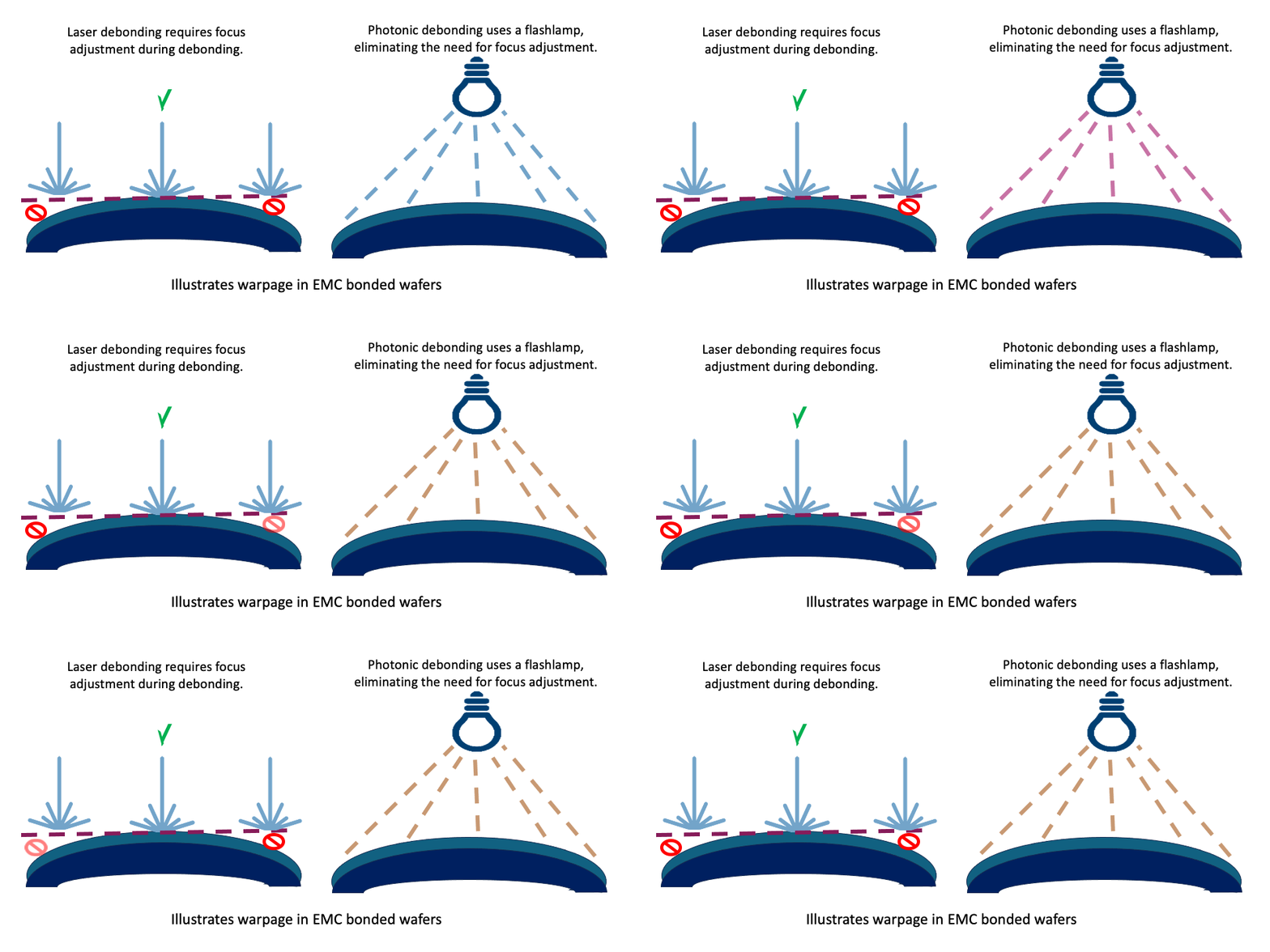
Applications: Photonic debonding is compatible with thinned device wafers less than 20 µm. It’s often desirable for bonded pairs that may have some slight bow/warp without causing inadequate debonding performance because of its high tolerance for variations in focal distance to the release layer. This release method also does not pose any threat or damage to the device, making it a more competitive option in comparison to laser debonding, and has faster throughput and lower cost of ownership.
Key Benefits of Photonic Debonding
Among the five debonding methods, photonic debonding proves to be most favorable in processes that require precision, such as wafer thinning and dicing. There are many benefits that demonstrate photonic debonding as a superior debonding method.
Lower Cost of Ownership
Since the flashlamp is more economical than a laser, the initial cost of ownership for photonic debonding is less than laser debonding. Additionally, the reusability of the glass carrier offsets the costs of single-use carriers. The cost of ownership can be reduced by over 30% with photonic debonding in comparison to other debonding methods.
Precision and Control
Photonic debonding often involves using specific wavelengths of light to target and break the bonds at the interface of materials. This targeted approach allows for precise control over the debonding process, potentially reducing damage to sensitive or fragile materials.
Successful on Warped Wafers
If wafers are concave or convex, photonic debonding still proves to be successful in debonding since emission is uniform up to 10 mm from the flash head.
Reduced Thermal Damage
Some laser debonding processes generate significant heat, which can cause thermal damage to the materials being processed. Photonic debonding might utilize wavelengths or energies that result in less heat generation, thereby reducing the risk of damaging the components.
Material Compatibility
Certain materials may respond better to specific wavelengths of light. Photonic debonding techniques can be optimized by choosing wavelengths that are more suitable for the materials involved, improving efficiency, and minimizing damage.
Selective Debonding
Photonic techniques can be fine-tuned to target specific layers or interfaces in a material stack, allowing for selective debonding without affecting other adjacent layers or components.
Process Efficiency
Depending on the application, photonic debonding methods might offer faster processing times or higher throughput compared to traditional laser debonding techniques.
Material consideration for a successful photonic debonding process
Photonic debonding is an ideal choice for wafer processors who seek to minimize cost, while achieving a clean debond process. Its scalability in wafer sizes, resistance to warped substrates, and tunability make it exceptionally versatile. The main consideration when electing to do a photonic debond process is to consider your material needs. You must ensure your materials have compatible adhesive properties and an optimized light-absorbing layer. For example, BrewerBOND® 305 material as an adhesive enables thinning to 50 µm, while only requiring a low-residue cleaning process enabling reuse of the carrier.
It’s important to note that the superiority of one method over another can heavily depend on the specific application, the materials involved, and the desired outcome. With over 40 years of experience innovating in the semiconductor wafer bonding and debonding field, Brewer Science has provided many customized solutions specific to our customers’ needs. While this guide serves as a high-level overview, we ask that you connect with us through the form at the bottom of the page so our expert team can provide you with the best solution considering your precision requirements, material characteristics, cost considerations, and the overall efficiency of the process for a particular application.


